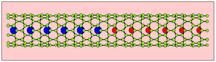
The conductance of the above tube using
a simple approximation to compute its transmission coefficient. The effective
voltage W is the sum of the applied voltage and potential difference at
the junction (internal voltage).
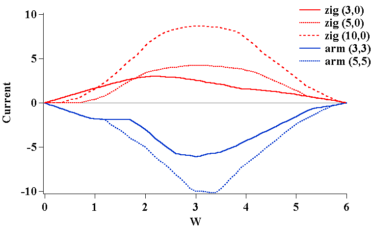
These are the non-linear I-V characteristics
of a few doped nanotubes. The calculated conductance is approximate ...
but one can notice the strong non-linear effect. (High bias results are
incorrect since in this calculation, we have only taken one p orbital per
atom, and therefore the DOS goes back to zero at higher energies.) The
I-W curve is odd with respect to the EFFECTIVE voltage W, but it is a non-symmetric
curve with respect to the applied bias voltage.
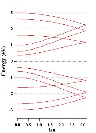
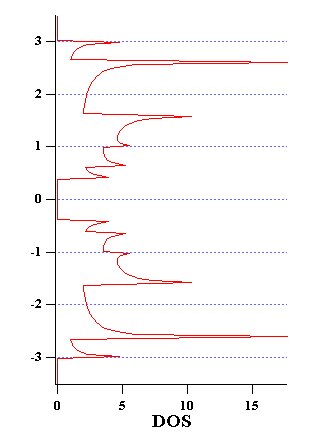
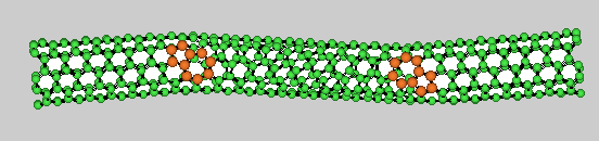
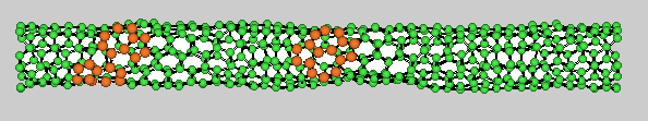
Defects (dislocations) in carbon nanotubess
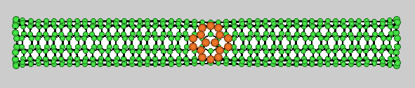
1 Stone-Wales transformation
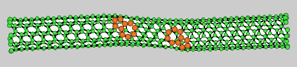
5 Stone-Wales transformations
10 Stone-Wales transformations
Molecular Dynamics of a streched
nanotube at 2000 K after 45 ps.